
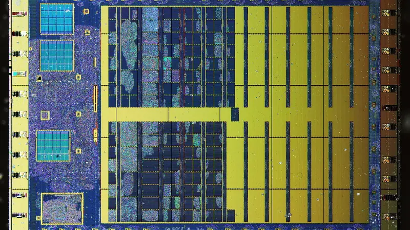
TYLsemi, a San Jose-based semiconductor startup, emerged from stealth on Tuesday with $43 million in early-stage funding to advance a chiplet platform for custom AI silicon. The company claims its standards-based connectivity, power and memory chiplets can reduce development time and cost by up to 50 percent for hyperscalers building specialized XPUs. Matter Venture Partners led the round, with Viola Ventures, GHOVC, Egis Technology and strategic investors participating, as reported by citybiz. Mohit Gupta, founder and CEO, said "The AI accelerator market is on track to reach $604 billion by 2033, and custom silicon XPUs built for specific hyperscaler workloads are the fastest-growing segment." This is a development to track on the AI chipmakers coverage hub.
Modular chiplets target custom XPU economics
TYLsemi's platform combines standards-based connectivity chiplets, power chiplets and memory chiplets with a customer's custom compute or fabric die. The TYL.IO connectivity family supports PCIe, ESUN and UALink, with a co-packaged optics roadmap, while TYL.Power is an integrated voltage regulator chiplet for in-package power efficiency. TYL.Mem memory connectivity is planned but details remain pending development. TYL.Forge bundles these chiplets with IP, foundry, packaging and production services, aiming to give hyperscalers a reusable foundation instead of a monolithic design. Engineering samples of TYL.IO and TYL.Power are expected in 2027 via TSMC.
Founded by Mohit Gupta and Sunil Bhardwaj, veterans of Alphawave, SiFive, Cadence and Rambus, TYLsemi is expanding engineering teams across silicon design, packaging and systems. The startup argues that UCIe die-to-die standard and mature 2.5D/3D packaging make chiplet design commercially practical. For infrastructure buyers, this matters because custom accelerators such as Google TPUs and AWS Trainium already compete with merchant GPUs for specific AI workloads; our training vs inference AI chips guide examines where bespoke silicon wins.
Yield, NRE and TCO arithmetic
Chiplet economics are driven by wafer cost and die size. Leading-edge wafer prices have risen from about $15,000 to $30,000 over five years, and dies at 500 to 600 mm² face worsening yield and timing closure. TYLsemi's illustrative estimate compares a monolithic 700 mm² 3nm chip at $350 million development cost and $3,000 unit price against a chiplet-based system with a 500 mm² 3nm compute die and four 100 mm² N-1 I/O chiplets, estimated at $150 million development cost and about $600 per SiP. At 100,000 units, the company estimates a 57 percent total cost of ownership reduction. However, TYLsemi stresses these are illustrative estimates, not actual manufacturing costs.
For chip design teams, the architectural implication is not just lower NRE: moving I/O, power management and eventually memory interfaces to reusable chiplets reduces the risk of integrating new process nodes and lets compute dies exploit the full reticle. Gupta told SiliconANGLE, "At that scale, chiplet-based design is no longer optional, yet there is no pure-play chiplet company serving this market with a full portfolio." The startup's TYL.Mem memory connectivity chiplet remains under development, so memory die selection and interface standards such as those governed by JEDEC Solid State Technology Association will be a key integration point for AI systems with high-bandwidth memory needs.
Deployment context and unknowns
TYLsemi says it has secured engagements with several tier-one customers, but has not named them, and TYL.Forge platform lead customers are being engaged. The first silicon, TYL.IO and TYL.Power engineering samples, will not arrive until 2027 via TSMC, which means early adopters need to design around a pre-silicon platform or wait for production-ready chiplets. TYL.Mem details are absent, leaving memory subsystem planning incomplete. The company targets AI accelerators, data-center CPUs, HPC, networking and heterogeneous SoCs, but the 2027 sample date and unannounced customer names leave a gap for infrastructure buyers evaluating whether to commit to custom silicon now or continue with merchant accelerators.
The chiplet approach also supports supply-chain resilience through modular, multi-source strategies. Meta has used a chiplet platform to build four XPU designs in two years, according to the funding announcement, a reference point for hyperscalers that want rapid iteration without full custom NRE. For teams weighing a bespoke XPU, practical considerations include evaluating standards compliance for UCIe, PCIe, UALink and ESUN, confirming advanced packaging options from foundries or OSATs, and checking memory chiplet availability against workload capacity planning. See the AI Chip Buyer’s Guide for more on accelerator selection criteria.
Architectural and deployment takeaways
- Modular chiplets reduce risk by isolating compute dies from I/O, power and memory chiplets, allowing smaller N-1 dies for I/O to improve yield.
- Standards-based connectivity (UCIe, PCIe, UALink, ESUN) and co-packaged optics roadmap support multi-source supply chains and avoid single-vendor lock-in.
- Integrated voltage regulation via TYL.Power can improve in-package power efficiency, but the memory chiplet (TYL.Mem) remains a planning dependency.
- The 2027 engineering sample timeline from TSMC means current designs must account for pre-silicon co-development or wait for qualified chiplets.
- TCO claims of 57 percent at 100,000 units depend on yield, packaging costs and memory pricing; treat the $350M vs $150M development cost figures as illustrative.